Logic gate symbols
Every gate in both standards: the ANSI distinctive shapes used on most American schematics, and the IEC rectangles used in European and formal documents. Same gates, two drawings.
The seven symbols
AND a ∧ b
High only when every input is high.
OR a ∨ b
High when at least one input is high.
NOT ¬a
Outputs the opposite of its single input.
XOR a ⊻ b
High when its two inputs disagree.
NAND ¬(a ∧ b)
The inverse of AND, and enough to build everything else.
NOR ¬(a ∨ b)
High only when every input is low.
XNOR ¬(a ⊻ b)
High when its two inputs agree.
Note that NAND is simply the AND shape with a bubble, and NOR is OR with a bubble. XOR is OR with one extra line across its back, which is easy to miss on a dense drawing, and XNOR is that shape with a bubble.
Side by side
The same gate in both standards, with the boolean expression and what the output does.
The bubble
One convention carries most of the meaning on a schematic: a small circle means invert.
- On the output, it negates the gate. AND becomes NAND, OR becomes NOR, and the NOT triangle is really just a buffer with a bubble.
- On an input, it means that pin is active low: the signal is inverted before the gate sees it. An AND with both inputs bubbled behaves as a NOR, which is De Morgan's law drawn rather than written.
- On a clock pin of a flip-flop, it means the part triggers on the falling edge rather than the rising one.
This is why experienced engineers redraw gates with bubbles moved around: pushing bubbles through a gate swaps AND for OR and often makes a schematic read more directly.
Which should I use?
If you are drawing for other people, match whatever they already use. American textbooks, datasheets and most schematic capture tools default to the ANSI shapes, and they have a real advantage: the outline tells you the function at a glance, even at small sizes or in a photocopy. IEC rectangles win when a part has many inputs or unusual behaviour, because there is always room for a label, and they are what international standards documents expect.
The simulator on this site uses neither. The editor draws every node as a labelled box, which is closer to IEC in spirit and keeps custom nodes and gates looking consistent.
Reference card
All seven gates in both standards on one image, for notes or a slide.
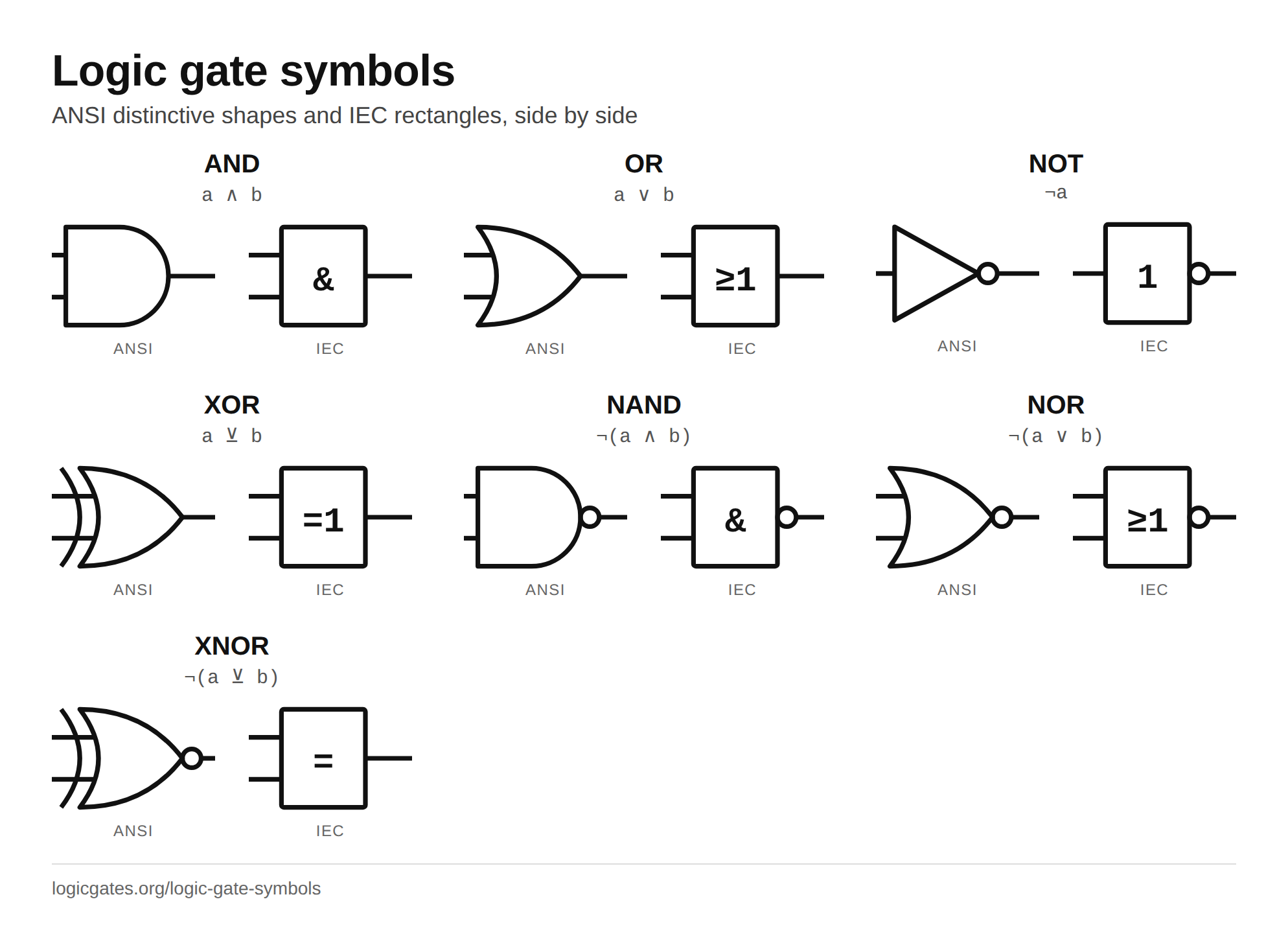 Click to download: Logic gate symbols chart
Questions
What is the difference between ANSI and IEC logic gate symbols?
The distinctive shapes give each gate its own outline: a D for AND, a shield for OR, a triangle for NOT. They come from MIL-STD-806 and are kept in ANSI/IEEE Std 91-1984, which is why they are usually just called the ANSI symbols — though that standard defines rectangular forms too. IEC 60617-12 uses one rectangle for every gate with a label inside saying what it does: & for AND, ≥1 for OR, 1 for a buffer, =1 for XOR. American schematics tend to use ANSI, European and formal standards documents tend to use IEC.
What does the little circle on a gate symbol mean?
That bubble means inversion. An AND with a bubble on its output is a NAND; an OR with one is a NOR; the triangle with a bubble is a NOT gate. A bubble on an input means that input is active low, so it is inverted before the gate acts on it.
How do I tell AND and OR apart?
The AND symbol has a flat back and a smooth semicircular nose, like a capital D. The OR symbol has a curved back and comes to a point. The trick people use is that AND is flat at the back, and OR is curved at both ends.
How is XOR drawn?
Exactly like OR, with a second curved line drawn just behind the back of the shape. That extra line is the only difference, so it is worth looking twice at a busy schematic. In IEC form the rectangle is labelled =1, meaning exactly one input is high.