SR latch and flip-flop
Set it, reset it, and it stays where you put it.
Live demo. Set the inputs, then clock it. Q⁺ = S ∨ (¬R ∧ Q)
Nothing clocked yet. The state only moves on an edge.
How it behaves
Raising S drives the output high and it stays high after S returns low. Raising R drives it back to 0. With both inputs low the circuit holds whatever it last had, and that holding is the whole point: it is the first circuit with memory rather than just a response to its current inputs.
Two NOR gates, each feeding one input of the other. The cross connection means each gate helps hold the other in place, so the pair has two stable configurations and sits in whichever one it was last pushed into. Raising both inputs at once is the flaw: it forces both outputs low, so the two "opposite" outputs are no longer opposite, and when the inputs drop together the result depends on which gate happens to be faster.
Characteristic table
What the next state is, for every combination of inputs and present state. The equation below is this table written as algebra.
| S | R | Q | Q⁺ | Effect |
|---|---|---|---|---|
| 0 | 0 | 0 | 0 | hold |
| 0 | 0 | 1 | 1 | hold |
| 0 | 1 | 0 | 0 | reset |
| 0 | 1 | 1 | 0 | reset |
| 1 | 0 | 0 | 1 | set |
| 1 | 0 | 1 | 1 | set |
| 1 | 1 | 0 | — | not allowed |
| 1 | 1 | 1 | — | not allowed |
Q⁺ = S ∨ (¬R ∧ Q)
That equation holds subject to S ∧ R = 0. It is written for the six rows that are allowed; at S = R = 1 the algebra says 1 while the real latch drives both outputs low, which is exactly why that input is ruled out rather than described.
Timing
The same behaviour in time rather than in a table. Each dashed line marks a clock cycle boundary — a rising edge, except for the last, which is just the end of the diagram — and Q only ever changes on an edge: that is what makes it a flip-flop rather than a latch. The inputs walk through every legal combination in turn, held for two cycles so you can see the response arrive a cycle late.
Reference card
The same waveform as an image, black on white, for notes or a slide.
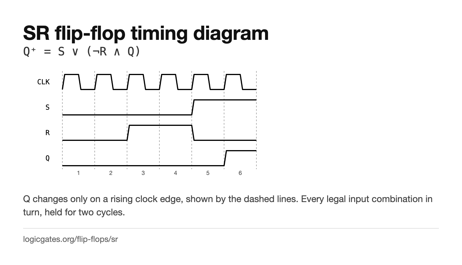 Click to download: SR flip-flop timing diagram
Excitation table
The same information turned around. You know the transition you want; this says what to put on the inputs to get it. This is the table you use when designing a counter or a state machine, and the X's are what make the driving logic small.
| Q | Q⁺ | S | R |
|---|---|---|---|
| 0 | 0 | 0 | X |
| 0 | 1 | 1 | 0 |
| 1 | 0 | 0 | 1 |
| 1 | 1 | X | 0 |
An X means the input does not matter for that transition, which is a don't care when you minimise the logic that drives it.
Building one
Two NOR gates, output of each into an input of the other. The free NOR inputs become S and R. Using NAND gates instead gives the same behaviour with active-low inputs, usually written S̄R̄.
The editor has a Delay node, which is what you need to make feedback settle predictably rather than oscillating.
Where it is used
- Debouncing a mechanical switch, where the two contacts set and reset the latch and the bouncing in between is ignored.
- The storage element inside every other flip-flop on this page: they are all an SR latch with logic bolted onto the front.
- Holding an alarm or fault condition until something explicitly clears it.
- Arbitrating between two requests, since whichever arrives first wins and holds.
Questions about the SR flip-flop
What is the difference between an SR latch and an SR flip-flop?
A latch responds the moment its inputs change. A flip-flop only looks at its inputs on a clock edge, so its output changes at predictable instants. An edge-triggered SR flip-flop is two gated SR latches in a master-slave pair on opposite clock phases, so the output can only move at the edge.
Why is S = R = 1 forbidden?
It drives both outputs low, so Q and its complement are momentarily equal, which the rest of the circuit does not expect. Worse, when the two inputs return to 0 together the latch settles into whichever state its gates happen to reach first, so the result is not predictable. The JK flip-flop exists largely to remove this case.